To Set Up A Common Base Transistor Circuit Project Pdf - Transistors as amplifiers and switches Our final topic of the term is an introduction to the transistor as a discrete circuit element. The basic CE circuit is shown in Figure 71.

Bipolar Transistor Tutorial The Bjt Transistor
Problem 1 Sketch the common-base output characteristic for the npn Bipolar Junction transistor in the shown circuit for IE02mA.
To set up a common base transistor circuit project pdf. DC power supply regulated double 0 - 30 V 1 Un 2. Before dismantling the circuit mark the transistor you used in some way for identification purposes. Both input emitter and output collector.
To change thus changing the Q-point of the transistor. Note that the midfrequency model assumes that the impedances due to C1 and C2 are negligible compared to the impedance of related components in the. 1To observe and draw the input and output characteristics of a transistor connected in common base configuration.
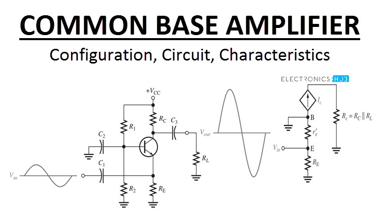
Common Base Configuration - has Voltage Gain but no Current Gain. Assume V CE 8 V R B 360 k and R C 2 k. Vary the collector-base voltage.
Measure the DC bias voltages on the base emitter and the collector. Since an integrated circuit is constructed primarily from dozens to even millions of transistors formed from a single thin silicon crystal it might be interesting and instructive to. Plot the resulting collector current waveforms.
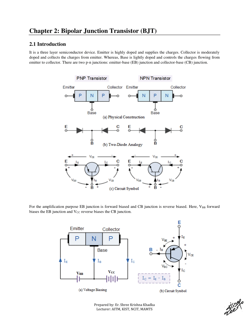
Common Emitter Configuration - has both Current and Voltage Gain. Set R L to be 1 k Ω and the supply voltage to 15V DC as shown in Figure 3. E-B junction is forward biased and C-B junction is reverse biased.
The emitter base junction is forward biased and collector base junction is reverse biased so that transistor remains in active region throughout the operation. Study of microwave components and set up a microwave bench pdf input output econometrics physics project to study the relation between input and output voltage and number of turns in a primary and secondary coil of common collector followed by a common base project for to set up a common base transistor circuit and to study its input and output characteristics and to. Name Quantity 1 Transistor BC 107 1 One 2 Resistors 1K 2 Two 3.
You started with simple resistive circuits then dynamical systems circuits with capacitors and inductors and then op-amps. Make sure the positive polarity of these capacitors are connected to the higher positive voltage in the circuit. To find α of the given transistor.
The common base terminology is derived from the fact that the base is common to both the input and output sides of the configurationThe base is usually the terminal closest toor atground potential. B Construct the dc load line and plot the Q-point. In next weeks lab we will use the 5V TTL transistor-transistor logic output of your function generator to drive a light bulb.
A RBE resistor connected between the base and emitter alleviates the influence of a dark current when operating at a high temperature. Theory Common Emitter amplifier has the emitter terminal as the common terminal between input and output terminals. Common application is to use a digital 0 or 5V signal with moderate impedance to control a device requiring a lot more power.
Common Collector Configuration - has Current Gain but no Voltage Gain. Download Full PDF Package. For normal operation the.
Breadboard 1 One Equipment. The figure below showing the notation and symbol used for npn transistor. Set the values of capacitors C1 C2 and C3 to 1µF each.
As its name suggests in the. Connect each set of points into a smooth line and mark each line with the appropriate base current 10. The circuit shown in Figure 10 B features a cascade connection of the grounded-base transistor Tr1 so.
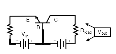
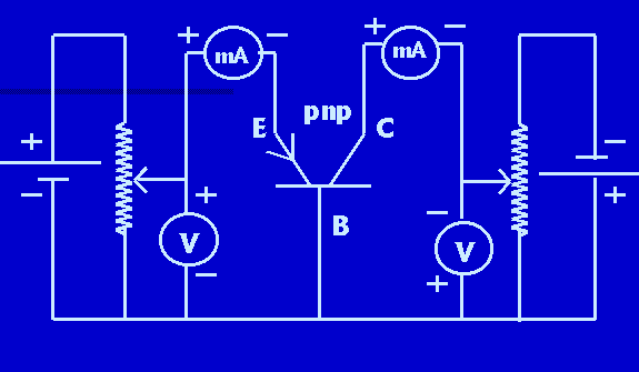
There are three section of transistor. Common Base Transistor Project AIM. The Common Base CB Configuration.
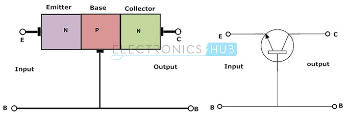
A transistor is a three terminal active device. Common Base Transistor Project - Free download as Word Doc doc docx PDF File pdf Text File txt or read online for free. The thickness of depletion layer is of the order of 10-6 m.
Perform this sweep for base currents IB 10 µA 30 µA 50 µA. The circuit of DC to DC c onversion is build with a ve ry popular IC LM555 used as multivibrator mood which generate required frequency range from 2. Diodes and Transistors 1.
Introduction So far in EE100 you have seen analog circuits. In designing a transistor switch you want most of the voltage drop to be across your device. Itle physics investigatory projects for class 12 cbse page link physics investigatory projects for class 12 cbse posted by gu rare and best chemistry investigatory projects class 12th cbse chemistry investigatory projects class 12th cbse physics investigatory projects for class 12 cbse to set up a common base transistor circuit and to study its input and output physics class 12.
Then you learned how circuit elements do. The circuit shown Figure 10 A uses a phototrans-istor with a base terminal. F Transistor A junction diode which is used for amplification is known as transistor.
In CB configuration the base is common to. Or grounded base configuration the. Figure 57 For Example.
The Basic Common Emitter Amplifier Figure 72 below is the small signal midfrequency incremental model corresponding to our CE circuit. This makes the base bias circuit extremely beta-dependent and very unstable. Verify your result using a simulation in PSpice.
Study the input and output characteristics of a transistor in Common Base Configuration. Connect the common base amplifier circuit you designed. To set up a common base transistor circuit and to study its input and output characteAsk Latest informationAbstractReportPresentation pdfdocpptto set up a common base transistor circuit and to study its input and output characte technology discussionto set up a common base transistor circuit and to study its input and output characte paper presentation details.
Digital ammeters 0 - 200 mA 2 Two. A In later experiments you will be using several transistors of the same type and you will have to identify the. A Determine the Q-point values of I C and V CE for the circuit in Figure 57.
![]()
Pdf A Common Base Linear Rf Power Amplifier For 3g Cellular Applications

Pdf A Common Base Linear Rf Power Amplifier For 3g Cellular Applications
The Common Base Amplifier Bipolar Junction Transistors Electronics Textbook

Common Base Amplifier Pdf Amplifier Electronic Circuits
![]()
Different Configurations Of Transistors Common Base Collector Emitter

Common Base Cb Configuration Or Common Base Amplifier
Pdf Bipolar Junction Transistor

Input Output Characteristics Of Cb Configuration And H Parameter Calculations Electronic Devices And Circuits Lab Vikramlearning Com
Different Configurations Of Transistors Common Base Collector Emitter
![]()
Pnp Transistor How Does It Work Use Arduino For Projects

Bjt Transistor Theory
Common Base Amplifier Configuration Circuit Characteristics
![]()
Different Configurations Of Transistors Common Base Collector Emitter
A Study Of Input Output And Transfer Characteristics Of A Transistor In Common Base Configuration
